Hardware
Table of Contents
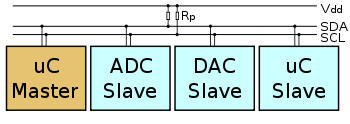
1 I2C
1.1 Characteristic
- multi-master serial single-ended computer bus
- used to attach low-speed peripherials to a motherboad,embedded system
- two bidirectional open-drain lines: Serial Data Line(SDA) and Serial Clock (SCL)
- support 100 kbit/s standard mode, 10 kbit/s low-speed mode, 400 kbit/s Fast mode and 3.4 Mbit/s High Speed mode.
1.2 Transfering data
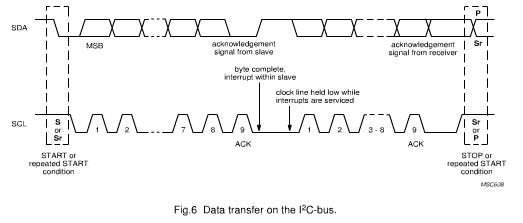
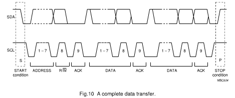
1.2.1 Byte format
Every byte put on the SDA line must be 8-bits long. The number of bytes that can be transmitted per transfer is unrestricfed. Each byte has to be followed by an acknowledge bit. Data is transferred with the most significant bit(MSB) first. if a slave can't receive or transmit annther complete byte of data until it has performed some other function, for example servicing an internal interrupt, it can hold the clock line SCL LOW to force the master into a wait state. Data transfer then continues when the slave is ready for another byte of data and releases clock line SCL. In some cases, it's permitted to use a different format from the I2C-bus format. Amessage which starts with such an address can be terminated by generation of a STOP condition, even during the transmission of a byte. In this case, no acknowledge is generated.
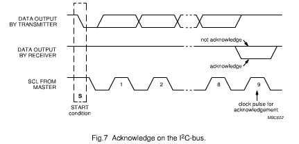
1.2.2 Acknowledge
Data transfer with acknowledge is obligatory. The acknowledge-related clock pulse is generated by the master. The transmitter releases the SDA line(HIGH) during the acknowledge clock pulse. The receiver must pull down the SDA line during the acknowledge clock pulse so that it remains stable LOW during the HIGH period of this clock pulse. Of course, set-up and hold times must alse be taken into account.

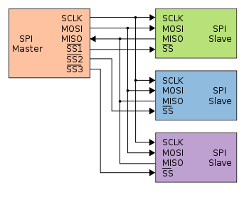
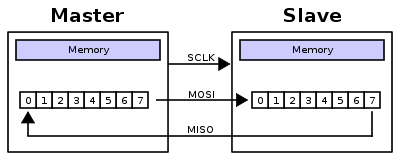
2 SPI(Serial Peripheral Interface Bus)
2.1 Characteristic
- synchronous serial data link standard
- operates in full deplex mode
- communicate in master/slave mode
- multiple slave devices are allowed with individual slave select lines.
- sometimes spi is called a four-wire serial bus
++ SCK: serial clock(output from master) ++ SDI: serial data in ++ SDO: serial data out ++ CS: chip select
++ Data Transmission
To begin a communication, the bus master first configures the clock, using a frequency less than or equal to the maximum frequency the slave device supports. Such frequencies are commonly in the range of 1–100 MHz.
The master then transmits the appropriate chip select bit for the desired chip to a logic 0. A logic 0 is transmitted because the chip select line is active low, meaning its off state is a logic 1; on is asserted with a logic 0. If a waiting period is required (such as for analog-to-digital conversion), then the master must wait for at least that period of time before starting to issue clock cycles.
During each SPI clock cycle, a full duplex data transmission occurs:
the master sends a bit on the MOSI line; the slave reads it from that same line
the slave sends a bit on the MISO line; the master reads it from that same line
Not all transmissions require all four of these operations to be meaningful but they do happen.
Transmissions normally involve two shift registers of some given word size, such as eight bits, one in the master and one in the slave; they are connected in a ring. Data is usually shifted out with the most significant bit first, while shifting a new least significant bit into the same register. After that register has been shifted out, the master and slave have exchanged register values. Then each device takes that value and does something with it, such as writing it to memory. If there is more data to exchange, the shift registers are loaded with new data1 and the process repeats.
Transmissions may involve any number of clock cycles. When there is no more data to be transmitted, the master stops toggling its clock. Normally, it then deselects the slave.
Transmissions often consist of 8-bit words, and a master can initiate multiple such transmissions if it wishes/needs. However, other word sizes are also common, such as 16-bit words for touchscreen controllers or audio codecs, like the TSC2101 from Texas Instruments; or 12-bit words for many digital-to-analog or analog-to-digital converters.
Every slave on the bus that hasn't been activated using its chip select line must disregard the input clock and MOSI signals, and must not drive MISO. The master must select only one slave at a time.
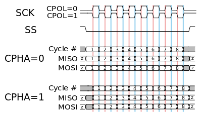
 ++ Clock polarity and phase
In addition to setting the clock frequency, the master must also configure the clock polarity and phase with respect to the data. Freescale's SPI Block Guide2 names these two options as CPOL and CPHA respectively, and most vendors have adopted that convention.
The timing diagram is shown to the right. The timing is further described below and applies to both the master and the slave device.
At CPOL=0 the base value of the clock is zero
For CPHA=0, data is captured on the clock's rising edge (low→high transition) and data is propagated on a falling edge (high→low clock transition).
For CPHA=1, data is captured on the clock's falling edge and data is propagated on a rising edge.
At CPOL=1 the base value of the clock is one (inversion of CPOL=0)
For CPHA=0, data is captured on clock's falling edge and data is propagated on a rising edge.
For CPHA=1, data is captured on clock's rising edge and data is propagated on a falling edge.
That is, CPHA=0 means sample on the leading (first) clock edge, while CPHA=1 means sample on the trailing (second) clock edge, regardless of whether that clock edge is rising or falling. Note that with CPHA=0, the data must be stable for a half cycle before the first clock cycle. For all CPOL and CPHA modes, the initial clock value must be stable before the chip select line goes active.
The MOSI and MISO signals are usually stable (at their reception points) for the half cycle until the next clock transition. SPI master and slave devices may well sample data at different points in that half cycle.
++ Clock polarity and phase
In addition to setting the clock frequency, the master must also configure the clock polarity and phase with respect to the data. Freescale's SPI Block Guide2 names these two options as CPOL and CPHA respectively, and most vendors have adopted that convention.
The timing diagram is shown to the right. The timing is further described below and applies to both the master and the slave device.
At CPOL=0 the base value of the clock is zero
For CPHA=0, data is captured on the clock's rising edge (low→high transition) and data is propagated on a falling edge (high→low clock transition).
For CPHA=1, data is captured on the clock's falling edge and data is propagated on a rising edge.
At CPOL=1 the base value of the clock is one (inversion of CPOL=0)
For CPHA=0, data is captured on clock's falling edge and data is propagated on a rising edge.
For CPHA=1, data is captured on clock's rising edge and data is propagated on a falling edge.
That is, CPHA=0 means sample on the leading (first) clock edge, while CPHA=1 means sample on the trailing (second) clock edge, regardless of whether that clock edge is rising or falling. Note that with CPHA=0, the data must be stable for a half cycle before the first clock cycle. For all CPOL and CPHA modes, the initial clock value must be stable before the chip select line goes active.
The MOSI and MISO signals are usually stable (at their reception points) for the half cycle until the next clock transition. SPI master and slave devices may well sample data at different points in that half cycle.
 Mode CPOL CPHA
0 0 0
1 0 1
2 1 0
3 1 1
Mode CPOL CPHA
0 0 0
1 0 1
2 1 0
3 1 1